WEEK 10
Activity:
- Construct and Development circuit to combine 2 source into 1 output.
Objective:
- Construct the circuit by using breadboard and test the circuit
- Construct and design using print circuit board (PCB).
- Test the circuit
 |
| Rectifier circuit by using diode |
 |
| Construct the circuit by using breadboard |
 |
| Design connection of the rectifier circuit |
 |
| Process of etching |
 |
Drilling
 |
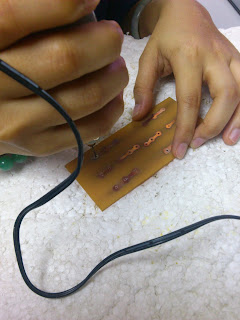
| Construct the component at the PCB |
 |
Process of solder the circuit
|
|
 |
| Full rectifier circuit |
for this week, the result for the rectifier circuit full fill the expectation expectation. The outputs Voltage from the PV and TE can be combine. The Value is more large when combine the two circuit.


No comments:
Post a Comment